| Поиск по каталогу |
|
(строгое соответствие)
|
- Профессиональная
- Научно-популярная
- Художественная
- Публицистика
- Детская
- Искусство
- Хобби, семья, дом
- Спорт
- Путеводители
- Блокноты, тетради, открытки
Properties of pure and doped wide-band gap semiconductor films.

В наличии
| Местонахождение: Алматы | Состояние экземпляра: новый |

Бумажная
версия
версия
Автор: Santosh Chackrabarti
ISBN: 9783330083028
Год издания: 2017
Формат книги: 60×90/16 (145×215 мм)
Количество страниц: 128
Издательство: LAP LAMBERT Academic Publishing
Цена: 33368 тг
Положить в корзину
| Способы доставки в город Алматы * комплектация (срок до отгрузки) не более 2 рабочих дней |
| Самовывоз из города Алматы (пункты самовывоза партнёра CDEK) |
| Курьерская доставка CDEK из города Москва |
| Доставка Почтой России из города Москва |
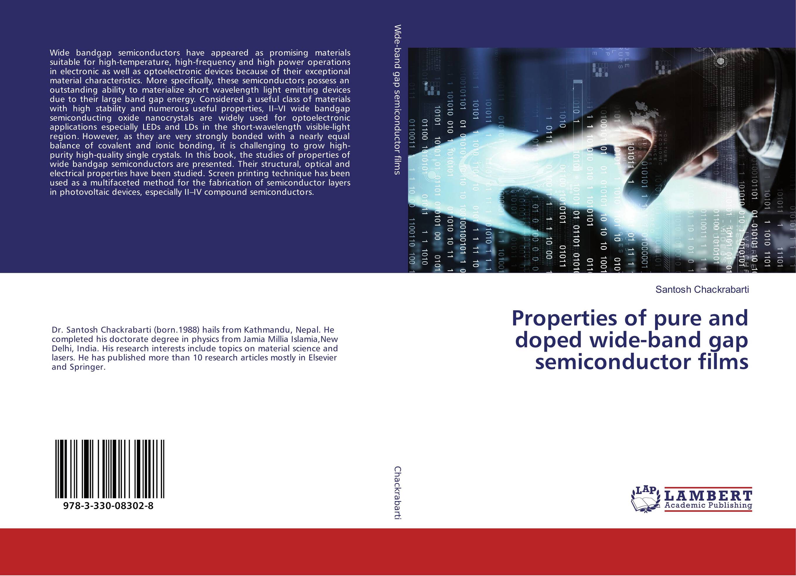
Аннотация: Wide bandgap semiconductors have appeared as promising materials suitable for high-temperature, high-frequency and high power operations in electronic as well as optoelectronic devices because of their exceptional material characteristics. More specifically, these semiconductors possess an outstanding ability to materialize short wavelength light emitting devices due to their large band gap energy. Considered a useful class of materials with high stability and numerous useful properties, II–VI wide bandgap semiconducting oxide nanocrystals are widely used for optoelectronic applications especially LEDs and LDs in the short-wavelength visible-light region. However, as they are very strongly bonded with a nearly equal balance of covalent and ionic bonding, it is challenging to grow high-purity high-quality single crystals. In this book, the studies of properties of wide bandgap semiconductors are presented. Their structural, optical and electrical properties have been studied. Screen printing technique has been used as a multifaceted method for the fabrication of semiconductor layers in photovoltaic devices, especially II–IV compound semiconductors.
Ключевые слова: doping, II-VI Semiconductors, Screen printing, wide band gap
Похожие издания
 | Отрасли знаний: Инженерные дисциплины -> Электротехника и электроника Suresh Pittala and S. Srinath Structural and Multiferroic Properties of Pure and RE Doped BiFeO3. Room temperature Multiferroics. 2014 г., 232 стр., мягкий переплет Multiferroics as multifunctional materials have stimulated much scientific and technological interest due to their potential applications. This book is the compilation of doctoral thesis of Suresh Pittala which deals with the synthesis and characterization of an interesting room temperature multiferroic material, bismuth ferrite (BFO) with and... | 47226 тг |


